

University Wafer Inc. Unveils Extensive Availability of Gallium Arsenide and Gallium Nitride Substrates
UniversityWafer, Inc.

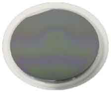
GaAs substrate
UniversityWafer, Inc. carriers hard-to-find Gallium Arsenide and Gallium Nitride Subsrates
SOUTH BOSTON, MA, UNITED STATES, January 10, 2024 /EINPresswire.com/ -- University Wafer Inc., a pioneering leader in the semiconductor substrate industry, proudly announces the expanded availability of high-quality Gallium Arsenide (GaAs) and Gallium Nitride (GaN) substrates. Catering to both academic research and large-scale industrial applications, the company is committed to meeting the growing demand for these essential materials in the semiconductor and electronics sectors in the face of Chinese export restrictions.Rising to the Challenge of a Dynamic Market
In an era marked by rapid technological advancements and heightened demand for efficient, high-performance electronic devices, University Wafer Inc. stands at the forefront of supplying critical materials. UniversityWafer, Inc's GaAs and GaN substrates, known for their superior electronic and photonic properties, are pivotal in driving innovations in various fields, including electric vehicles, telecommunications, aerospace, and renewable energy.
Unmatched Quality and Versatility
University Wafer Inc.’s GaAs substrates offer exceptional electron mobility and a direct bandgap, making them ideal for high-frequency and opto-electronic applications. Their unique properties enable the production of high-efficiency solar cells, laser diodes, and ultra-fast electronic components. Substrates with Gallium Nitride are renowned for their high thermal conductivity and ability to operate at high voltages and temperatures, making them indispensable in power electronics, LED technology, and cutting-edge radar systems.
Meeting Diverse Customer Needs
Understanding the diverse needs of all clients small and large. University Wafer Inc. offers GaAs and GaN substrates in various dimensions, dopant types, and orientations. UniversiyWafer, Inc along with partnering plants state-of-the-art manufacturing facilities ensure the highest quality standards. UniversityWafer, Inc's team of experts is dedicated to providing customized solutions to meet specific research and production requirements.
Small and Large Quantity Orders with Global Reach
Whether for small-scale experimental setups or large-scale production lines, University Wafer Inc. is equipped to handle orders of any size. Both small and large quantities are not a problem, thus ensuring that researchers, startups, and multinational corporations alike have access to the substrates they need. With a global distribution network, we guarantee timely and secure delivery products to any location worldwide.
Commitment to Sustainability and Ethical Sourcing
University Wafer Inc. commitment to sustainability ensures that all materials are sourced ethically and responsibly. UniversityWafer, Inc. actively collaborate with suppliers who share a vision for environmental stewardship and adhere to strict standards for responsible mining and processing practices.
Collaboration with Academia and Industry
University Wafer Inc. is not just a supplier but a collaborator in the advancement of science and technology. We partner with academic institutions and industry leaders to support research and development initiatives, offering technical consultation and customized solutions that push the boundaries of what is possible in semiconductor technology.
Customer-Centric Approach
University Wafer Inc., maintains long-term relationships provides clients and partner plants with fast responsive customer service, technical support, and commitment to understanding and fulfilling various clients' needs.
Looking Ahead: Embracing the Future of Semiconductor Technology
As the semiconductor industry evolves, University Wafer Inc. is poised to meet its future challenges and opportunities. We continuously invest in research and development to enhance product offerings and keep pace with the latest technological advancements.
Invitation to Connect
UniversityWafer, Inc. invites researchers, developers, and industry professionals to explore the range of GaAs and GaN substrate inventory and discover how University Wafer Inc. can contribute to their next groundbreaking project. For more information about UniversityWafer, Inc. products and services, please visit https://order.universitywafer.com or contact UniversityWafer, Inc. directly.
About University Wafer Inc.
University Wafer Inc., based in Boston, Massachusetts, is a leading provider of semiconductor substrates for the global electronics industry. With a focus on innovation and quality, the company offers a wide range of materials, including silicon, silicon carbide, sapphire, and more, to meet the evolving needs of the technology sector.
Christian Baker
UniversityWafer, Inc.
+1 617-268-2595
email us here
Visit us on social media:
Facebook
Twitter
LinkedIn
EIN Presswire does not exercise editorial control over third-party content provided, uploaded, published, or distributed by users of EIN Presswire. We are a distributor, not a publisher, of 3rd party content. Such content may contain the views, opinions, statements, offers, and other material of the respective users, suppliers, participants, or authors.